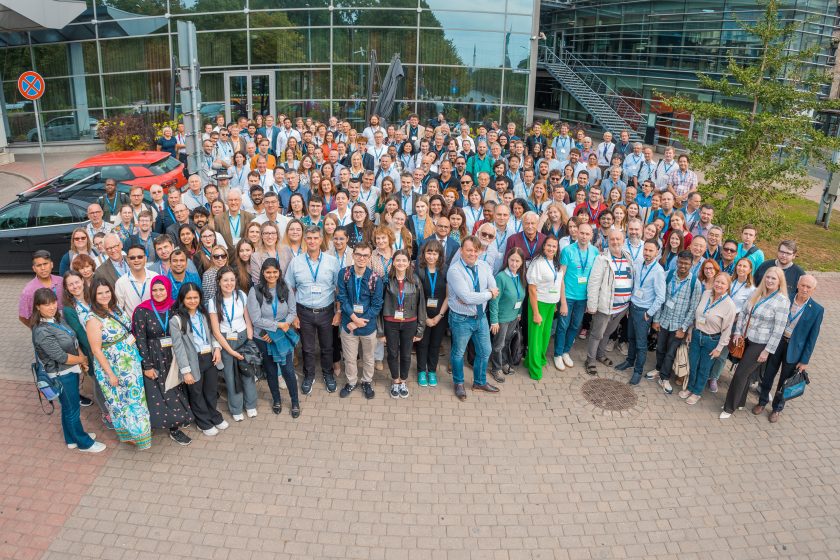
We were honoured to be part of the co-organising team of the largest international conference dedicated to nanomaterials research. Dr Modris Greitans, Director of the Institute, opened the international conference “Nanomaterials: Applications & Properties”. As Honorary Chairman of the Conference Organising Committee, he represented not only EDI but also the Latvian Academy of Sciences. In his speech, the Director of the Institute encouraged the guests to take the opportunity to enjoy the beautiful city of Riga and Latvia.
Both institutions are also co-organisers of the conference. The conference was dedicated not only to the discovery and exploration of new nanomaterials but, very importantly, to their various applications, in order to exploit the unique physical and chemical properties of these materials for practical purposes. An intensive programme from 9 to 13 September featured a variety of presentations on this topic.
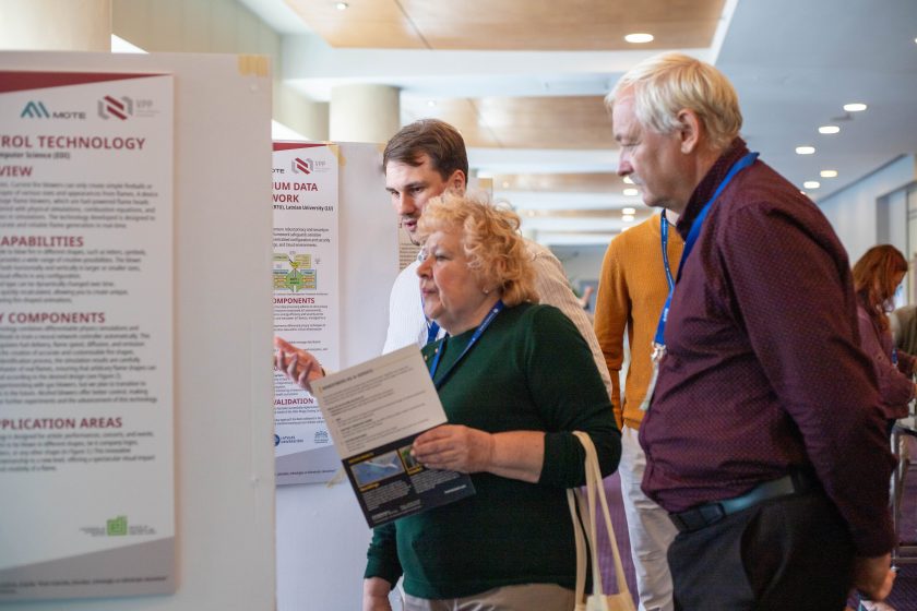
During the breaks, participants could actively network and learn about the scientific achievements of partners, including EDI. As this topic is related to the research themes of the Institute of Electronics and Computer Science – development of smart sensors and actuators, data processing, the transformation of nanomaterials into smart nanomaterials involving artificial intelligence.
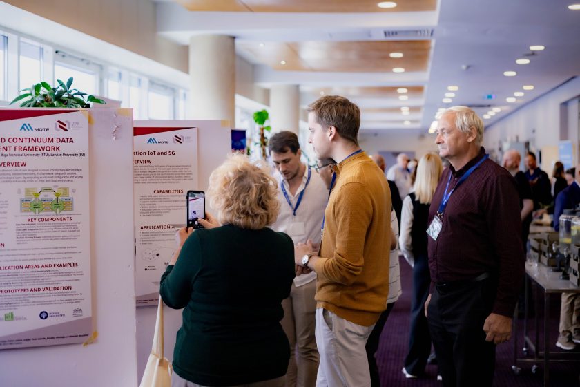
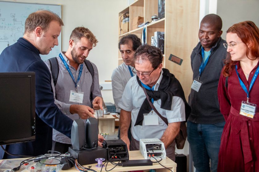
EDI presented the work of the project “Ecosystem for Smart Materials, Photonics, Technology and Engineering”. In this project, the Institute is responsible for the fourth work package: “ROBOTICS/IoT” (RoLISe). This work package focuses on three technology groups identified for their high added value for industry: robotics, Internet of Things (IoT) and smart sensor systems. Visitors had the opportunity to get more in-depth information on the achievements and to get to know the Latvian science developed by EDI scientists.
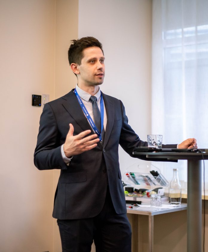
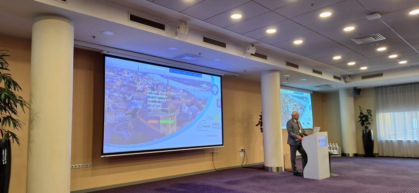
We are particularly proud that our Senior Researcher Rihards Novickis gave a presentation on the development of a quantum sensor based on diamonds with NV centre impurities. The diamond sensor, based on a nitrogen vacancy, provides unprecedented measurement accuracy and has been shown to be a transformative sensing tool for the study of electrical, magnetic and thermal properties.
The technology has already found many applications in research, such as imaging nanoscale nonlinear spin textures, optical detection of resonant spin wave modes, non-invasive measurement of ferromagnetic materials, 2D analysis of magnetic materials, millimetre-scale mapping of charge current distributions and many other applications. Showing the advantages and challenges of these methods.
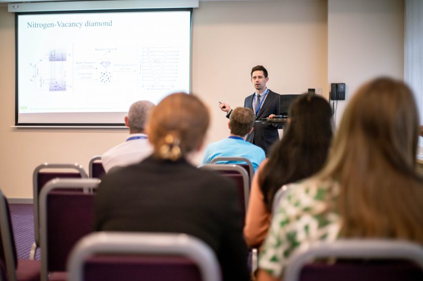
It also gives an overview of current EU projects contributing to the development of quantum sensors. And how EDI is using its unique past experience working with physicists to improve the applicability of new sensor technology.
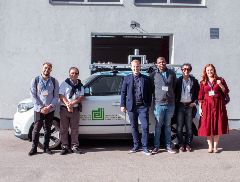
To give the guests the opportunity to get to know Latvia’s leading scientific institutions, excursions were organised, including to EDI. The guests were welcomed by Dr Kaspars Ozols, Deputy Director for Development. The guests were introduced to all 5 EDI laboratories, including the laboratory headed by Dr. Rihards Novickis, where they could already see and discuss in more detail the achievements presented the previous day.